
Hi,
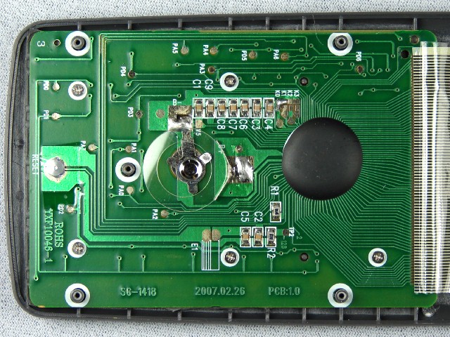
I have a device here that i would like to do a little experiment with. I believe it is made with a bare 'chip'
rather than a chip inside a package and this bare chip is covered with a black blob that appears to be
epoxy or something similar. Im pretty sure this is a Chip-On-Board solution.
What i would like to try is removing part of the black blob. Not the whole thing, but just part of it
perhaps. I'd like to see what can be done with it once part of the black blob is removed.
Especially, i'd like to access some of the pins for possible rewiring.
What would be nice is if someone here already tried this and has had at least some success.
Alternately if that isnt possible, some ideas on this subject.
Thanks...
Suggestions for removing black 'blob'
Suggestions for removing black 'blob'
LEDs vs Bulbs, LEDs are winning.
-
SETEC_Astronomy
- Posts: 582
- Joined: Tue May 09, 2006 12:44 am
- Contact:
Re: Suggestions for removing black 'blob'
Perhaps this will be of some use to you http://camerahacks.10.forumer.com/viewtopic.php?t=1021
-
Janitor Tzap

- Posts: 1707
- Joined: Sat Aug 12, 2006 5:17 pm
- Contact:
Re: Suggestions for removing black 'blob'
Try a hot air heat gun.
Or better, a Hot Air SMD removal station with variable heat temperature.
Signed: Janitor Tzap
Or better, a Hot Air SMD removal station with variable heat temperature.
Signed: Janitor Tzap

Re: Suggestions for removing black 'blob'
The best info I've ever seen on this subject was from Bomarc Services. Unfortunately, I don't recall
where this was posted; I guess it wasn't here at N&V forums. I suggest you get in touch with them
and ask for their advice. They seem to have lots and lots of experience in this area.
where this was posted; I guess it wasn't here at N&V forums. I suggest you get in touch with them
and ask for their advice. They seem to have lots and lots of experience in this area.

Re: Suggestions for removing black 'blob'
COB (chip-on-board) heralded the end of conventional packages in many applications in cheap consumer electronics products. Attach the semiconductor die to the PCB, wire bond from the chip pads directly down to the copper traces on the board, add blob and cure. Fini.
If you dissolved the epoxy blob, you'll find .001" gold or aluminum wires going from the chip top to the PCB. Rather fragile wires!
In short, your mission is nearly impossible if you want the circuit to stay intact with the blob removed. The epoxy doesn't "un-desolve" chemically.
However, if circuit operation isn't critical, a destructive method I've used may work, just to get a look at whats in there: drip hot sulphuric acid on the blob, about one a second, and the acid will slowly dissolve the binders in the blob. Slow, dangerous, smelly, and of course dissolves most eveything around it too.
Do it under a fume hood or outside!
WA2RBA
Re: Suggestions for removing black 'blob'
The only other thing I can think of is a suggestion by Don Lancaster in an old
Resource Bin column - a dental x-ray. He was dealing with a potted circuit, so
that was a different circumstance. But perhaps it could provide unseen pins &
dimensions which you could use to (gently) attack it with a file/dremel/x-acto.
Resource Bin column - a dental x-ray. He was dealing with a potted circuit, so
that was a different circumstance. But perhaps it could provide unseen pins &
dimensions which you could use to (gently) attack it with a file/dremel/x-acto.

Re: Suggestions for removing black 'blob'
After the epoxy blob of the COB (chip-on-board)
http://www.rskey.org/%7Emwsebastian/rev ... 39_pcb.jpg
is removed with a special solvent (available), you would see this:
http://www.ocularlcd.com/images/COBcircuit.jpg
Miguel
http://www.rskey.org/%7Emwsebastian/rev ... 39_pcb.jpg
is removed with a special solvent (available), you would see this:
http://www.ocularlcd.com/images/COBcircuit.jpg
Miguel
- Abolish the deciBel ! -
Re: Suggestions for removing black 'blob'
Hello again,
Thanks much for all the great ideas. I am starting to get an idea how
hard this would be to accomplish and it is starting to look like it
is nearly impossible partly because i dont want to have to spend all
day on one repair/modification and partly because i dont want to get
involved with the kinds of chemicals needed for this kind of thing.
Also, i dont even know if the chip(s) have leads (small wires or
otherwise) or they have little bumps on the bottom to make the
connections, which would complicate matters even more and probably
render most techniques impossible.
jwax:
Thanks for the detailed explanation. I think that sums it up quite
well in that most likely the end product will no longer be usable.
I wanted to make modifications but of course still have the circuit
working in the end.
sofaspud:
Well, i dont have daily access to an x-ray machine so that's that.
If i knew where to attack the circuit i might try a Dremel, but
i dont even know where the pin(s) are yet that i want to work with.
I guess i would have to figure that out too somehow.
Externet:
Hey, thanks for those pictures! Those are the very pics i was hoping
for so i could see roughly what i was looking for under the blob.
I can see now that it may not be possible to do what i want to do.
It looks like i would have to contact the manufacturer to get the
complete construction details so i would know before hand where to
dig. I would bet they are not willing to give out that info.
LEDs vs Bulbs, LEDs are winning.
Re: Suggestions for removing black 'blob'
Hi John. One of a few that show up on search:jwax wrote:I'll bite- what special solvent?
http://www.hisglassworks.com/cart/cart. ... etail&p=99
There is another way of searching under "potting compound solvent" ; perhaps methylene chloride?
Miguel
- Abolish the deciBel ! -
Re: Suggestions for removing black 'blob'
Packaged semiconductors are routinely dismantled in a generalMrAl wrote: What i would like to try is removing part of the black blob. Not the whole thing, but just part of it
perhaps. I'd like to see what can be done with it once part of the black blob is removed.
Especially, i'd like to access some of the pins for possible rewiring.
...
What would be nice is if someone here already tried this and has had at least some success.
Alternately if that isnt possible, some ideas on this subject.
process called "decap". There are numerous service bureaus
locally (Silicon Valley) that do this work.
A popular method is "jet etch" to remove the epoxy fill without
damage to the die or bond wires. Usually this is in preparation
for TEM (Tunneling Electron Microscopy) of the die, or de-processing
for FA (failure Analysis), reverse engineering, and competive analysis.
Read more here

Re: Suggestions for removing black 'blob'
Having worked as or with F/A engineers for over 20 years, jwax and bigglez have it essentially right.
For a manual decap the usual method typically entails using a dermel to shape a pocket over the die then placing the thing on a hot plate and dripping either 250C sulphuric acid or red fuming nitric acid works better or fuming sulphuric acid also works well. The procedure requires periodic rinsing with water but if you don't completely dry the part with alcohol (100%, not that cheap drug store stuff) and bake it for a while, the residual water will react with the acid and destroy any exposed copper. Most labs will use the jet etch decapper because it is safer and more controlled.
Its kind of an art. In most labs, these decaps are left to an experienced wet lab technician but most F/A engineers have done at least some. Lately I have seen some decapped parts for mobile phones. The die inside is impossibly thin 100um and is quite flexible and easy to break. COB parts are a bear to decap due to the not flat shape of the packaging material. To make matters worse, the die is face up and its easy to nick a bond wire when routing the top cavity. Done properly though, the device can remain functional. Most labs will charge between $250 and $500 to decap a part and provide you with a few microscope digital photos.
Going a little further, ceramic IC packages are usually hollow inside and can be opened by grinding with a diamond faced grinding disc until the package is thinned and you can see the outline of the cavity window. Then you apply sticky tape and rip the thinned lid off like you were waxing a leg (not that I have ever done that).
BTW, F/A is a fascinating career for those of you who are good with physics, chemistry and electronics (lets not forget report writing) at the same time (very cross-trainable). These guys get to use the most expensive tools in the company very often. It's like CSI for chips and passives.
There are some organic solvents that may work but they will destroy the FR4 substrate faster than the COB cover epoxy. http://www.dynaloy.com/ Unfortunately this stuff is about as expensive as the decap service would cost. PM me if you want a recommendation for a F/A lab in your area. I'm well hooked up in this industry.
Its pretty sure bet that all the pins are already wired out to the PC board and that there is nothing you can do to alter the chip underneath unless you have a FIB (Focused Ion Beam/Electron Microscope). Not sure if the latest breed of talking hallmark cards use flash or still use ROM to store the music. Anything else is likely not reconfigurable.
Re: Suggestions for removing black 'blob'
Agreed! More so when the parts in question are counterfeit.haklesup wrote: BTW, F/A is a fascinating career for those of you who are good with physics, chemistry and electronics (lets not forget report writing) at the same time (very cross-trainable). These guys get to use the most expensive tools in the company very often. It's like CSI for chips and passives.
Several examples of "wrong die" or "fraudulent die" or "bogus
package markings" have come across my desk. There are
financial incentives to strip and remark some garbage parts,
dump them in the broker market for cash as the hottest parts,
and run...
More so in the early 2000s when an industry IC shortage and
the "dot com" bubble were present.

Re: Suggestions for removing black 'blob'
Can you please post some part numbers of those items that crossed your desk? I heard that many Analog Devices parts were being counterfeited in the "early 2000s". AD likes to make single source parts and because of that, charge "through the nose" for replacements.Bigglez wrote:More so when the parts in question are counterfeit. Several examples of "wrong die" or "fraudulent die" or "bogus package markings" have come across my desk. There are
financial incentives to strip and remark some garbage parts, dump them in the broker market for cash as the hottest parts, and run...
More so in the early 2000s when an industry IC shortage and the "dot com" bubble were present.
-=VA7KOR=- My solar system includes Pluto.
Re: Suggestions for removing black 'blob'
Sorry, to post proprietary info would be unethical. Many of theseBob Scott wrote:Can you please post some part numbers of those items that crossed your desk? I heard that many Analog Devices parts were being counterfeited in the "early 2000s". AD likes to make single source parts and because of that, charge "through the nose" for replacements.
cases become evidence for civil cases (I don't know of any criminal
cases - most of the counterfeiters are offshore). Also, its
embarrasing for the legit semi houses to have FA parts that
are wrongly branded, remarked with in-range date codes,
are reject-bin sorted, or even have the wrong die in the
package!
Most of the issues were created by greed during the dot-com
shortages, but also include older analog products built on
obsolete processes. The part numbers lived much longer than
the process - some were redesigned, die-shrunk, or sub-con
built off shore. Die shrink is the normal business model for
digital (and some high volume descretes), but less so for RF
and high performance analog parts.
The chip business looks a lot different from the vendor's
point of view...
But, good news! Flat panel TVs, cell phones, PCs, DVRs,
and other consumer items are so cheap now that repair or
upgrades are not needed. Just toss them out after one or
two years and get the next gen.
Who is online
Users browsing this forum: No registered users and 17 guests